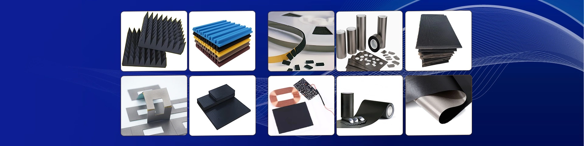
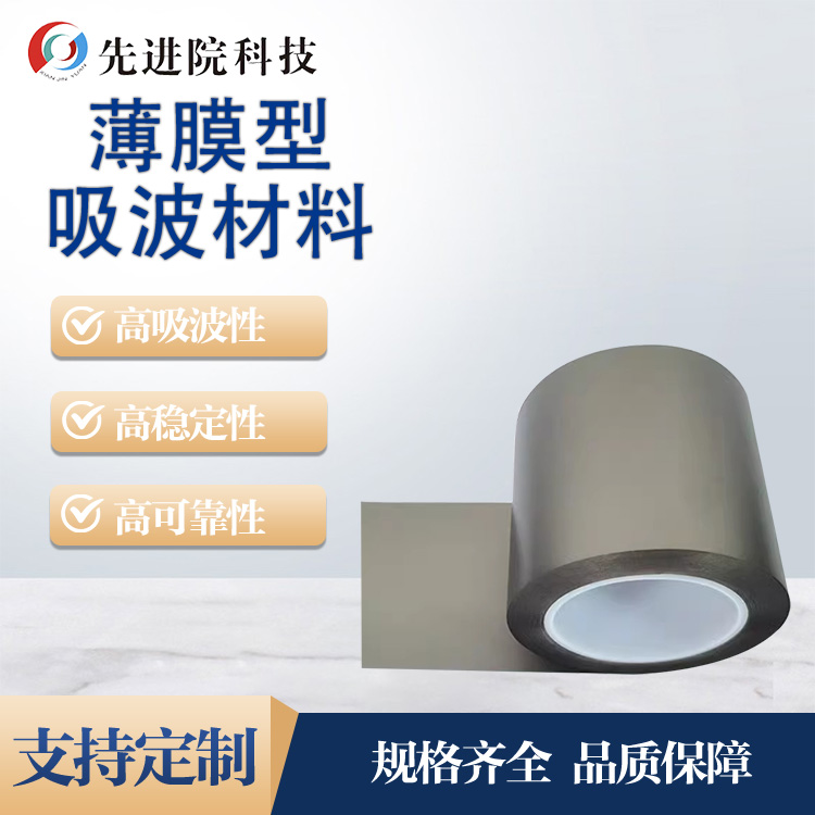
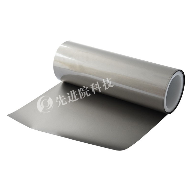
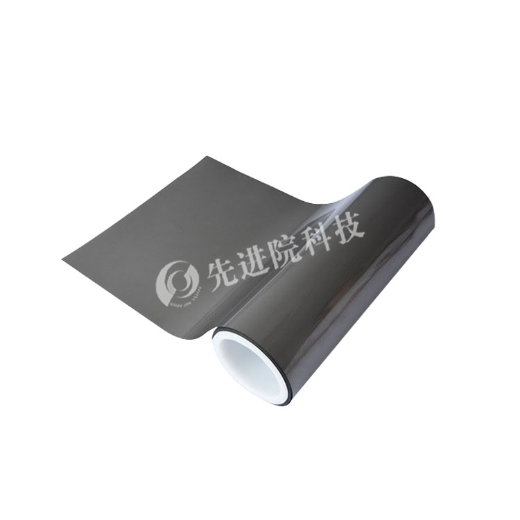
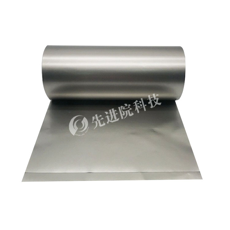
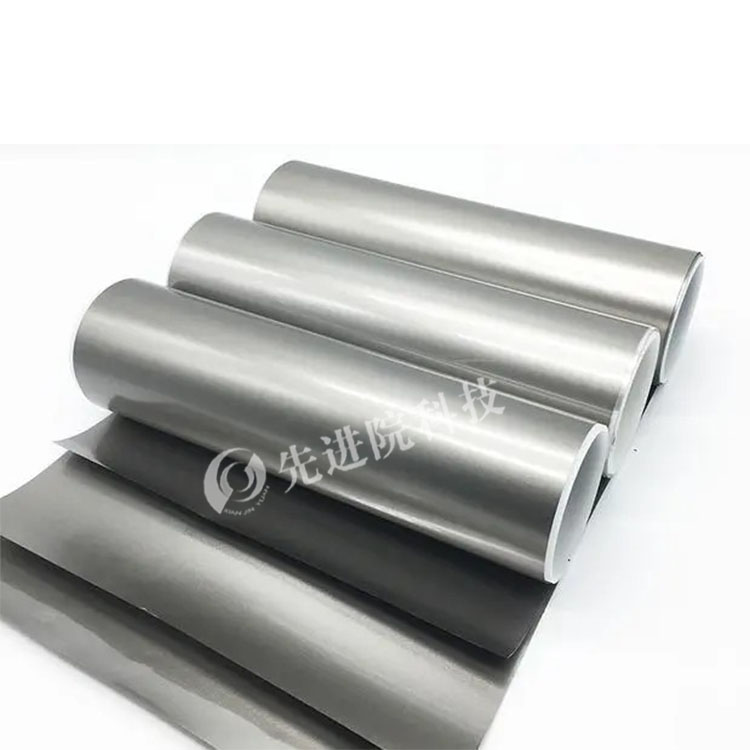
Thin film absorbing materials are a special type of material that have excellent electromagnetic wave absorption capabilities and are characterized by thin thickness and light weight.
Definition and Composition
Thin film absorbing materials are mainly prepared by special processes using flexible polymer materials and high magnetic permeability materials. This material is capable of absorbing electromagnetic wave energy projected onto its surface and converting it into other forms of energy (such as thermal energy), thereby reducing the reflection and transmission of electromagnetic waves.
Type and Characteristics
There are various types of thin film absorbing materials, each with its unique characteristics and properties:
- Magnetic thin film absorbing materials, such as ferrite thin films, have high magnetic permeability and dielectric constant, and can absorb electromagnetic waves through magnetic and dielectric losses. This type of material performs well in the low-frequency range and is an ideal choice for low-frequency RFID applications such as RFID.
- Metal based composite thin film absorbing material: Metal (such as nickel, cobalt, etc.) is combined with other materials to form a thin film, which achieves the function of absorbing waves through conductivity loss, magnetic loss, and other effects. This type of material has excellent conductivity and mechanical properties, making it suitable for applications that require high strength and conductivity.
- Nanostructured thin film absorbing materials: Due to the quantum size effect and surface effect of nanoparticles, nanostructured thin film absorbing materials have special absorption properties for electromagnetic waves. For example, carbon nanotube films exhibit excellent absorption performance in specific frequency bands due to their unique structure and electrical properties. This type of material exhibits excellent absorption performance in the high frequency range and is the preferred choice for high-frequency RFID applications such as 5G communication and satellite navigation.

Working principle
The working principle of thin film absorbing materials is mainly based on their special electromagnetic properties and absorption mechanism. When electromagnetic waves are projected onto the surface of a material, the magnetic particles and polymer matrix inside the material will interact, converting electromagnetic wave energy into thermal energy or other forms of energy and dissipating it. In this way, the propagation of electromagnetic waves inside the material is hindered, reducing the reflection and transmission of electromagnetic waves, thereby reducing electromagnetic interference.
Application scenarios
Thin film absorbing materials are widely used in various scenarios that require reducing electromagnetic interference and improving electromagnetic compatibility, such as:
- RFID system: Using thin film absorbing materials around the antennas of RFID tags and readers can reduce the reflection and transmission of electromagnetic waves, improve the reading accuracy and stability of RFID systems.
- Communication equipment: Thin film absorbing materials are used in communication devices such as mobile phones, digital cameras, and laptops to suppress multiple reflections of electromagnetic waves, absorb chaotic echoes, eliminate interference and influence of microwaves on various components, and improve the human-machine environment.
- Aerospace: In the aerospace field, thin film absorbing materials can be used to reduce the electromagnetic radiation generated by aircraft and satellites during high-speed flight, improving their stealth performance.
- Military field: In the military field, thin film absorbing materials can be used to produce equipment such as stealth fighter jets and stealth missiles, improving combat effectiveness.


 en
en