
Hotline:0755-22277778
Tel:0755-22277778
Mobile:13826586185(Mr.Duan)
Fax:0755-22277776
E-mail:duanlian@xianjinyuan.cn
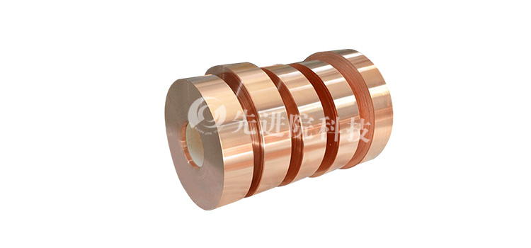
PBN substrate copper plated filmIn all applications of PCB, the thickness of copper foil can be customized according to requirements and adjusted based on the different thicknesses of the substrate. The application of copper foil on PCB can be divided into two categories: electroplated copper foil and substrate free copper plating.
Electroplated copper foil:
Electroplated copper refers to the process of depositing a thin metal film with a thickness of 0.5-1.0 micrometers on a metal surface through chemical methods. Electroplated copper is mainly used for printed circuit boards, circuit board components, and electronic components, which can provide corrosion resistance, oxidation resistance, insulation, and conductivity.
No substrate copper platingIt refers to the direct use of chemical methods to make the metal surface of PCB into a conductive metal film without any electroplating process, mainly used as a conductive layer in printed circuit boards and electronic components.
The non substrate copper plating commonly used is electroplated copper foil, which is a copper metallization film deposited from copper ions. Electroplated copper foil is typically 0.5-1.0 microns thick and is commonly used for printed circuit boards, circuit board components, and electronic components.

Due to the significant resistance between the PCB metal substrate and electronic components, insulation treatment is necessary to reduce their resistance coefficient and thus lower the resistance value. In order to reduce the resistance of printed circuit boards, it is usually necessary to coat a layer of chemical copper on the metal substrate, which forms a chemical copper layer on the surface of the substrateInsulation film (copper network)This reduces the resistance coefficient of the circuit.
Compared with traditional electroplating or chemical plating, the advantages of using non substrate copper plating film for insulation treatment are:
1. Copper network formed on the substrate surface without electroplating or chemical copper plating film;
Due to its excellent properties, non substrate copper plated films have been widely used in the PCB industry in recent years.
Application scope of non substrate copper plating technology:
1. Substrate free copper plating technology is mainly applied in the PCB industry and can be used to manufacture some special structured PCB products.
2. Substrate free copper plating technology can be used to produce some precision electronic products, such as electronic connectors, which can replace traditional copper foil to reduce the contact resistance between signal lines and circuit boards, thereby improving product performance.
3. Substrate free copper plating technology can be used to produce high-density multi-layer PCB products, such as high-density interconnect (HDI) boards.
4. The substrate free copper plating technology can also be used to produce some multifunctional PCB products, such as wearable devices, which have the characteristics of good flexibility and foldability.
There are still many problems in the development of substrate free copper plating technology, such as:
1. The substrate free copper plating technology has caused serious pollution to the environment and is currently widely used in the PCB industry;
2. The technology of copper plating without substrate has problems such as high cost and poor stability;
3. The copper plating solution without substrate is unstable and contains many impurities;
4. The technology of copper plating without substrate still has problems such as long electroplating cycle and low electroplating efficiency.
Currently the most advancedNo substrate copper platingThe technology involves directly coating a substrate free copper plating solution onto a PCB metal substrate, followed by chemical electroplating (similar to traditional chemical copper plating solutions) after cleaning, rather than using traditional electroplating methods.


Advanced Institute (Shenzhen) Technology Co., Ltd, © two thousand and twenty-onewww.avanzado.cn. All rights reservedGuangdong ICP No. 2021051947-1 © two thousand and twenty-onewww.xianjinyuan.cn. All rights reservedGuangdong ICP No. 2021051947-2