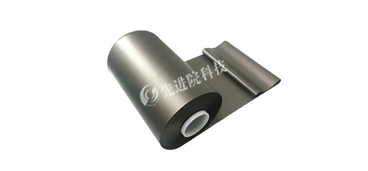
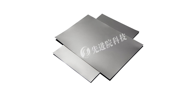
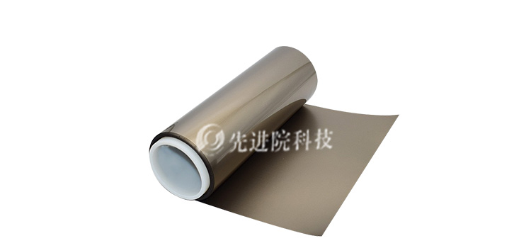
The importance of electromagnetic compatibility and stealth technology is increasingly prominent in modern electronic and military equipment. Thin film absorbing materials, as a key electromagnetic protection material, can effectively absorb electromagnetic waves, reduce reflection and transmission, thereby reducing the electromagnetic radiation of equipment and improving stealth performance. However, the reflection of electromagnetic waves at material interfaces has always been a key factor affecting absorption performance. This article will explore how thin film absorbing materials can overcome this problem, and specifically introduce the research and development of Advanced Institute (Shenzhen) Technology Co., Ltd
Research Platinum Brand Thin Film Absorbing Materials.
1、 Reflection of electromagnetic waves at interfaces
When electromagnetic waves are incident on the interface of different media, due to the sudden changes in the electromagnetic parameters of the media (such as dielectric constant and magnetic permeability), some electromagnetic waves will be reflected back to the original medium, while others will be transmitted into the new medium. This reflection phenomenon not only reduces the absorption efficiency of electromagnetic waves, but may also lead to electromagnetic interference between devices. Therefore, reducing the reflection of electromagnetic waves at the interface is the key to improving the performance of absorbing materials.
2、 Factors affecting reflection
1. Sudden changes in electromagnetic parameters
The sudden change in electromagnetic parameters is the main cause of reflection. When electromagnetic waves are incident from air (low electromagnetic parameters) onto absorbing materials (high electromagnetic parameters), significant reflections occur due to sudden changes in electromagnetic parameters. Therefore, it is necessary to optimize the electromagnetic parameters of the material and gradually change them to reduce reflection.

2. Material thickness
The thickness of the material can also affect reflection. Although thicker materials can increase the propagation path of electromagnetic waves and improve absorption efficiency, they may also increase reflection. Therefore, it is necessary to find a suitable thickness that matches the impedance of the material with the characteristic impedance of free space and reduces reflection.
3. Surface structure of materials
The surface structure of materials, such as roughness and coating, can affect the incidence and reflection of electromagnetic waves. By designing special surface structures, such as pyramid or cone structures, multiple reflections and absorption of electromagnetic waves can be increased, thereby reducing reflections.
3、 Strategies to overcome reflection problems
1. Optimize electromagnetic parameters
By adjusting the composition and structure of the material, its electromagnetic parameters can be optimized to gradually change and reduce the reflection of electromagnetic waves at the interface. For example, adding conductive fillers such as carbon black and metal powder can increase the conductivity of the material, thereby reducing surface impedance. At the same time, choosing soft magnetic materials with high permeability (such as iron silicon aluminum alloy, iron nickel alloy) can improve the permeability of the material and further optimize impedance matching.
2. Optimize the thickness of materials
Through experiments and simulations, the optimal thickness of the material can be determined. Generally speaking, the thickness of the material should be designed to be a multiple of the electromagnetic wavelength (such as 1/4 wavelength or 1/2 wavelength) to achieve optimal impedance matching. For example, for 10GHz electromagnetic waves, the thickness of the material can be designed to be 7.5mm (1/4 wavelength) or 15mm (1/2 wavelength) to reduce reflection and improve absorption efficiency.

3. Design special surface structures
By designing special surface structures, such as pyramid or conical structures, multiple reflections and absorption of electromagnetic waves can be increased. These structures can effectively reduce the reflection of electromagnetic waves, allowing more electromagnetic wave energy to enter the interior of the material, thereby improving the absorption performance. For example, the surface of a pyramid shaped structure can increase the path length of electromagnetic waves, allowing them to reflect and absorb multiple times on the material surface, thereby improving the absorption efficiency.
4. Use multi-layer structure design
Multilayer structure design can effectively optimize impedance matching. By combining materials with different electromagnetic parameters, the impedance of electromagnetic waves can be gradually adjusted to approach the characteristic impedance of free space. For example, high permeability soft magnetic layers can be alternately stacked with high dielectric constant dielectric layers to form a multi-layer composite structure. When electromagnetic waves are incident on this structure, they will reflect and refract multiple times between different layers, increasing the propagation path and loss of electromagnetic waves inside the material, thereby improving the absorption efficiency in the low-frequency range.
4、 Innovative achievements of Advanced Institute (Shenzhen) Technology Co., Ltd
Advanced Institute (Shenzhen) Technology Co., Ltd. has achieved significant results in the research and production of thin-film absorbing materials. The company adopts advanced material selection, process optimization, and structural design technologies to ensure
Research Platinum Brand Thin Film Absorbing MaterialsPerformance stability in long-term use. Specific innovative achievements include:
1. Optimize electromagnetic parameters
The company uses high-performance absorbing fillers such as carbon nanotubes, graphene, metal powders, etc. These materials have high specific surface area and good electromagnetic parameters, which can effectively absorb electromagnetic wave energy. By precisely controlling the type and amount of fillers added, the electromagnetic parameters of the material were optimized to achieve efficient absorption performance over a wide frequency band.
2. Optimize the thickness of materials
The company has determined the optimal thickness of the material through experiments and simulations. Generally speaking, the thickness of the material should be designed to be a multiple of the electromagnetic wavelength (such as 1/4 wavelength or 1/2 wavelength) to achieve optimal impedance matching. For example, for 10GHz electromagnetic waves, the thickness of the material can be designed to be 7.5mm (1/4 wavelength) or 15mm (1/2 wavelength) to reduce reflection and improve absorption efficiency.

3. Design special surface structures
The company adopts advanced micro nano processing technology and designs special surface structures, such as pyramid shaped or conical structures. These structures can effectively reduce the reflection of electromagnetic waves, allowing more electromagnetic wave energy to enter the interior of the material, thereby improving the absorption performance. For example, the surface of a pyramid shaped structure can increase the path length of electromagnetic waves, allowing them to reflect and absorb multiple times on the material surface, thereby improving the absorption efficiency.
4. Use multi-layer structure design
The company adopts a multi-layer structural design, combining materials with different electromagnetic parameters together to form a multi-layer composite structure. By alternately stacking high permeability soft magnetic layers with high dielectric constant dielectric layers, the impedance of electromagnetic waves can be gradually adjusted to approach the characteristic impedance of free space. When electromagnetic waves are incident on this structure, they will reflect and refract multiple times between different layers, increasing the propagation path and loss of electromagnetic waves inside the material, thereby improving the absorption efficiency in the low-frequency range.
5、 Conclusion
Thin film absorbing materialIn overcoming the reflection problem of electromagnetic waves at interfaces, the absorption performance can be significantly improved by optimizing electromagnetic parameters, optimizing material thickness, designing special surface structures, and using multi-layer structural designs. Advanced Institute (Shenzhen) Technology Co., Ltd. ensures the stability and reliability of research platinum brand thin-film absorbing materials in various complex environments through a series of innovative technologies, providing strong support for electromagnetic protection of electronic and military equipment. In the future, with the continuous advancement of technology, thin film absorbing materials will demonstrate their enormous application potential in more fields.
The above data is for reference only, and specific performance may vary due to production processes and product specifications.
