
Hotline:0755-22277778
Tel:0755-22277778
Mobile:13826586185(Mr.Duan)
Fax:0755-22277776
E-mail:duanlian@xianjinyuan.cn
Thick film substrates have been widely used in fields such as hybrid integrated circuits, RF devices, and power devices due to their short preparation process, simple film formation process, and high reliability. But due toFilm-forming slurryThe limitations of the characteristics and film formation methods of thick film substrates based on printing technology inevitably result in poor line edge pattern accuracy, large line width/spacing, and poor uniformity and density of large-area film layer thickness, which limits their application in high-precision, high fidelity, and low loss signal characteristic fields such as optoelectronic conversion, radio frequency (RF), and microwave circuits.
Compared to low-frequency circuits, conductors play an additional role as microstrip transmission lines in high-frequency circuits. Considering the influence of the radio frequency resistance and skin depth of conductors, high conductivity, good line edge and line accuracy, film thickness greater than 3-4 times skin depth, good high temperature resistance and adhesion are required for the substrate metal conduction band. The traditional thin film process has good line conductivity, high accuracy, and edge quality, but there are difficulties in increasing the thickness of the film layer (usually 1 μ m). Although it is possible to increase the thickness of the film layer through electroplating technology, there is a significant difference in resistivity between different film layers, resulting in poor adhesion at high temperatures and relatively high costs, which limits its application in high-frequency signal and other fields. Exploring new film layer patterning methods based on traditional thick film technology has become a hot research topic.
At present, the main methods for thick film patterning with fine lines are precision printing and laser engraving. By adjusting the mesh size of the wire mesh and adjusting parameters such as viscosity of the auxiliary slurry, it is possible to produce thick film lines with a characteristic line width/spacing of 50 μ m/50 μ m. However, there are defects such as poor uniformity of line thickness, low production efficiency, and easy breakage of lines, which limit their large-scale application. The laser engraving method can quickly achieve the preparation of thick film micro lines, with high line accuracy and edge quality. However, there are defects such as poor removal quality of large-area film layers and poor insulation between lines caused by the reaction between laser and substrate (such as AlN), which limit its application in the production of thick film substrates with low line density. This article studies the process technology of producing thick film micro lines based on thin film lithography/etching methods. By introducing photolithography methods, high-precision, high fidelity, and feature line width/spacing of 45 μ m/45 μ m micro lines in the thickness direction of the film layer are achieved, successfully solving the contradiction between film thickness and accuracy, and realizing the production of high-precision wiring thick film substrates
Principle and Characteristics of Thick Film Gold Conductor Photolithography Process
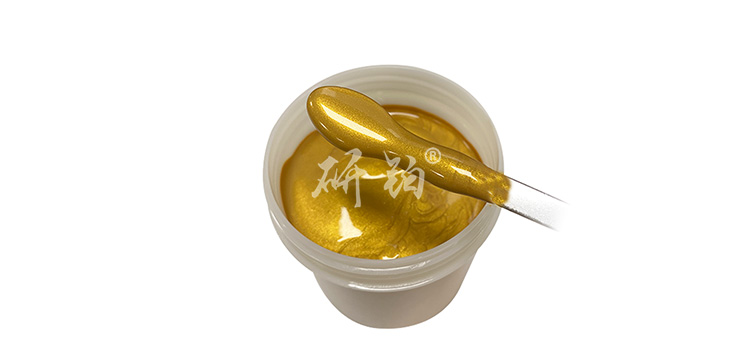
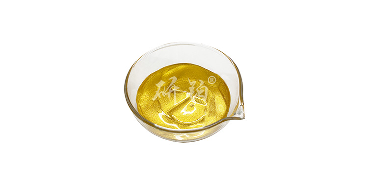
Thick film lithography technology is the direct coating of additional photosensitive resin materials or photoresist on the entire surfaceSintered gold conductorAfter baking, the substrate surface is exposed and developed to form a corrosion mask, and then the gold film layer in the required pattern area is removed by wet etching method to form fine wiring. In this process, the determination of etching solution and photoresist is interrelated. The selected etching solution should not cause damage to the photoresist, so that the circuit pattern can be selectively corroded under the protection of the photoresist. The corrosion should be clean and the line accuracy should meet the requirements. The selected photoresist has good photosensitivity and strong corrosion resistance, suitable for deep corrosion processing requirements, without drilling and floating of the photoresist. The technical roadmap related to thick film lithography is shown in Figure 1.

For the cleaned bare substrate: 1) Apply a thick film printing method to the front surface of the substrate for coatingGold pasteThen, the high reliability of gold film formation can be achieved through sintering process; 2) Coating photoresist on the surface of the substrate after film formation to achieve complete coverage of the metal film layer, avoiding defects such as pinholes, micropores, and detachment caused by incomplete coverage during subsequent corrosion processes. Baking, exposing, and developing the photoresist on the thick film substrate coated with photoresist according to the thin film lithography process to achieve the production of a photoresist mask on the surface of the thick film substrate; 3) The removal of thick film layer is achieved through wet etching method, and after de gluing and cleaning, a thick film substrate with fine wiring is formed; 4) Evaluate the processing quality and reliability of the prepared thick film substrate. Compared to traditional paste printing for film formation, thick film lithography for producing fine lines has the following characteristics.
1.1 High precision thick film wiring
Due to the high accuracy of mask preparation using photolithography, the line width/spacing of thick film lines prepared by photolithography is naturally better than that obtained by screen printing. due toGold pasteAfter sintering, graphic production is carried out, effectively avoiding the problem of graphic shrinkage in the traditional slurry sintering process and improving the accuracy of thick film wiring lines.
1.2 Better uniformity of film thickness and surface quality
In the technology of preparing thick film micro lines based on photolithography,Gold pasteThe entire surface is coated on the substrate, avoiding the influence of screen printing and unreasonable printing parameter settings on the thixotropic properties and casting of the slurry, greatly improving the uniformity of film thickness and surface quality.
1.3 Good edge quality of thick film lines
Based on the corrosion process, the production of lines avoids burrs on the edges of lines caused by paste adhesion, collapse, etc. during the printing process, effectively improving the quality of thick film wiring line edges.
Key technologies for photolithography of thick film gold conductors
2.1 High quality corrosion-resistant thick film layer production technology
For the special requirements of photolithography/corrosion, it is required that the surface roughness of the thick film layer formed is low, and the thickness uniformity of the film layer within the substrate area is good. Through comparative research on screen printing parameters, it was verified thatGold pasteThe length of flow has a significant impact on the quality of the film-forming film layer.
2.1.1 Effect of leveling time on film thickness
Under the premise of fixed slurry model, substrate size, and printing parameters, the influence of different flow level lengths on the wet film thickness of slurry at different positions on the substrate was studied. The target thick film wet film thickness is 20 μ m, and the relevant results are shown in Figure 2.
It can be seen that as the leveling time prolongs, the thickness difference of the wet film of the slurry at different positions on the same substrate gradually decreases. At the same time, the thickness uniformity of wet films sintered at different leveling times follows a similar pattern, indicating that appropriate leveling time can help improve the thickness uniformity of printed wet films and sintered films, as well as control subsequent wet corrosion parameters and the amount of line side drilling.
2.1.2 Effect of leveling time on surface roughness of film formation
Under the premise of a certain slurry model, substrate size, and printing parameters, the influence of different flow lengths on the surface roughness (protrusion) of the wet film on the substrate was studied, with a target thick film wet film thickness of 20 μ m.


Advanced Institute (Shenzhen) Technology Co., Ltd, © two thousand and twenty-onewww.avanzado.cn. All rights reservedGuangdong ICP No. 2021051947-1 © two thousand and twenty-onewww.xianjinyuan.cn. All rights reservedGuangdong ICP No. 2021051947-2