1. Introduction
To learn alone without friends is to be ignorant and ignorant;
2. Background introduction
During the certification testing of shielding material www.avanzado.cn for a certain controller product, communication failure and system crash occurred due to ESD ± 6KV contact discharge. It needs to be restarted to recover. Analysis and rectification are carried out to address this issue.
3. Analysis and rectification
3.1 Controller networking and experimental points
The schematic diagram of controller networking and ESD discharge points is shown in Figure 1.
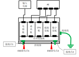
(a) Schematic diagram of networking and discharge points
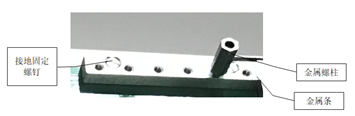
(b) Physical image of discharge point
Figure 1 Controller networking and experimental points
3.2 Experimental phenomena
ESD contact discharge is ± 6KV. When conducting tests on discharge points 1 and 2 (about 3-6 discharges per point), as well as discharge point 3 (about 10-20 discharges per point), communication failures will occur, making it impossible to communicate with the upper computer and resulting in a system crash that needs to be restarted for recovery. There are no issues with the discharge point 4 test.
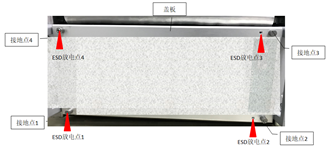
3.3 Grounding reliability investigation
3.3.1 Grounding point impedance measurement
Using a multimeter to measure the impedance of the cover plate grounding point, the results are as follows:
Table 1 Grounding Impedance
| Cover plate grounding point |
Ground Impedance |
notes |
| Grounding point 1 |
0.2-0.3Ω |
The grounding impedance is high and the grounding effect is poor |
| Grounding point 2 |
0.2-0.3Ω |
| Grounding point 3 |
0.1-0.2Ω |
High grounding impedance and poor grounding effect |
| Grounding point 4 |
0-0.1Ω |
Generally acceptable |
Note: When the ESD spectrum reaches the GHz frequency band, using a multimeter to measure the impedance value of the chassis grounding may not be accurate, but it can be used as a preliminary qualitative analysis and judgment.
3.3.2 Investigation of chassis grounding point change
Manually change the grounding point position of the controller and conduct ESD experiments on each discharge point to verify the reliability of each grounding point. The detailed results are shown in Table 2.
Table 2 Experimental results of changing the grounding point of the chassis
| Cover plate discharge point |
experimental result |
| Initial experimental grounding configuration |
Discharge point 1 |
Fail |
| Discharge point 2 |
Fail |
| Discharge point 3 |
Fail |
| Discharge point 4 |
Pass |
| Grounding point change: Near Grounding Point 2 |
Discharge point 1 |
Fail |
| Discharge point 2 |
Pass |
| Discharge point 3 |
Pass |
| Discharge point 4 |
Pass |
| Grounding Point Change: Near Grounding Point 1 |
Discharge point 1 |
Pass |
| Discharge point 2 |
Fail |
| Discharge point 3 |
Fail |
| Discharge point 4 |
Pass |
3.3.3 Summary of Grounding Reliability Investigation
(1) After the grounding point position was changed to 2, there were no issues with the discharge points 2/3/4 experiment, but discharge point 1 still caused communication failure and system crash; After the grounding point position was changed to 1, there was no problem with the discharge point 1/4 experiment, but the discharge point 2/3 still caused communication failure and system crash.
(2) Poor overlap between the cover plate and the chassis ground, with high impedance at grounding points 1/2/3, and acceptable impedance at grounding point 4;
(3) The overall overlap design between the controller cover plate and the chassis is unreliable, leading to problems during ESD testing.
3.4 Analysis of Communication Failure and System Crash Caused by Poor Grounding
3.4.1 ESD coupling mechanism analysis
3.4.1.1 ESD waveform parameters
The waveform parameters of ESD discharge current in IEC61000-4-2 standard are shown in Figure 2 [1], and the peak discharge current of 6KV is 22.5 (1 ± 15%) A.
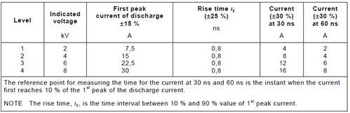
Figure 2: Waveform Parameters of Contact Discharge Current
3.4.1.2 ESD Spectrum Characteristics
The discharge current and spectral characteristics of 6KV level ESD are shown in Figures 3 and 4 [2]. The amplitude of ESD is generally between 0-1.2 GHz, and above 1.2 GHz, the amplitude basically decays to 0. There are two peaks during the entire frequency period. Between 0-30 MHz, the amplitude gradually decays and decays quickly. Then, as the frequency increases to 60 MHz, the amplitude reaches the second peak, and as the frequency continues to increase, the amplitude gradually decays to 0.
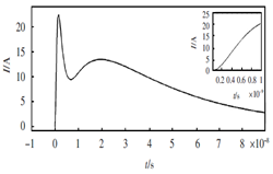
Figure 3 6KV discharge current waveform
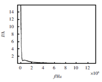
Figure 4 6KV Contact Discharge Current Spectrum
3.4.1.3 Analysis of ESD discharge coupling mechanism
(1) ESD interference mode
ESD interferes with controllers through common mode interference, mainly in the following forms:
The field coupling formed during ESD discharge generally occurs when the grounding point is good, but there is a sensitive signal or wiring near the grounding position:
ESD discharge current forms noise voltage Vnoise in the grounding impedance path, which interferes with sensitive equipment and generally occurs in situations with poor grounding and high grounding impedance;
The direct injection of ESD discharge current into sensitive signals usually occurs during ESD injection experiments on pins.
(2) Structural analysis:
The structural hierarchy of the controller cover plate grounding: cover plate fastening spring screws → metal bolts → metal strips → grounding fixing screws → chassis grounding. The PCB via has no grounding copper plate, and there is no overlap with the metal strip and the chassis. The overlap between the metal strip and the casing is only done through threads, which is unreliable and has high impedance. The structural grounding is shown in Figure 5.
(a) Physical picture of the grounding point of the cover plate
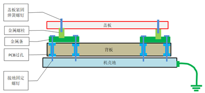
(b) Schematic diagram of the grounding structure of the cover plate
Figure 5: Grounding Structure of Cover Plate
(3) Analysis of Interference Path and Equivalent Mechanism Circuit
When the grounding between the cover plate and the chassis is good, the impedance is low enough to form an equipotential overlap with the chassis without any voltage difference.
The main discharge paths of ESD are ① and ② in Figure 6. Due to the close grounding physical path of ①, most of the interference will flow from the ① path to the ground. The interference field formed by the current flowing through path ① can interfere with sensitive signals or sensitive wiring in the surrounding area.
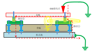
Figure 6 Schematic diagram of ESD discharge path
When the grounding connection between the cover plate and the chassis ground is poor (with high impedance), the ESD discharge current will form a noise voltage Vnoise at the connection point.
The noise voltage passes through the distributed capacitance between the cover plate and the PCB board, forming interference current that flows through the PCB, causing interference to the sensitive dry signal, as shown in Figure 7.
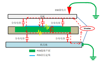
Figure 7 Schematic diagram of ESD coupling mechanism with poor grounding
 en
en 


