AbsorberIt is a composite material with excellent absorption ability for electromagnetic waves. This type of absorbing material is a composite material formed by physically refining and magnetic field processing an alloy to form a high permeability magnetic alloy, and uniformly dispersing it in a polymer.
Principle and structure of absorbing materials
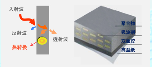
1. The principle of absorbing materials is based onMagnetic microwave absorberAs the main body, the electromagnetic waves emitted by electronic devices are converted into thermal energy through insulation loss, magnetic loss, and impedance loss to reduce electromagnetic radiation. It has the characteristics of high magnetic permeability, wide frequency band selection, and can be developed specifically for specific frequency bands.
2. Absorbing materials have good absorption characteristics in the range of 10MHz~6GHz, which can avoid electromagnetic interference or leakage caused by secondary reflection. The main products areType of absorbing patchIt can also be processed into various shapes according to customer needs. Absorbing materials can be used inside electronic device cavities such as laptops, mobile phones, and communication cabinets.
3. Absorbing materials have good electromagnetic wave absorption effect, wide absorption frequency, and can be customized according to customer requirements for frequency bands. They are thin in thickness, cost-effective, and have a wide range of uses and applications.
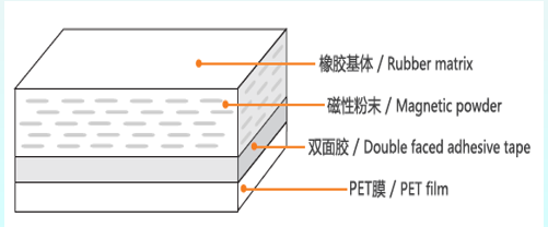
Principle and Structure Diagram of Absorbing Materials
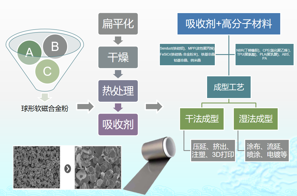
Product production process
Application of the product
1. Can be used inside electronic device cavities such as laptops, mobile phones, and communication cabinets.
2. Can be used to reduce radiation and noise from various electronic devices.
3. Can reduce coupling, conduction, and radiation interference between low frequencies, as well as minimize low-frequency echo interference
4. Can reduce internal EMI (resonance, crosstalk) within the barrier frame.
5. Applied between chips and heat dissipation modules.
6. Application of EMI/RFI: EMI(Electro Magnetic Interference): The literal translation is electromagnetic interference The three elements of electromagnetic interference are interference source, interference propagation path, and sensitive equipment Interference sources refer to electronic devices or systems that generate electromagnetic interference, which can propagate through cables, space, etc. Sensitive devices refer to electronic devices or systems that are easily affected by electromagnetic interference. RF Interference: RF is a high-frequency alternating current, commonly known as electromagnetic waves Radio frequency interference is the interference caused by electromagnetic waves Two electromagnetic waves with similar frequencies will be simultaneously received by the receiver, causing interference There will be harmonic interference near the launch pad Interference with other receiving devices Transmitting electromagnetic waves of the same frequency can interfere with radio stations
 en
en 


