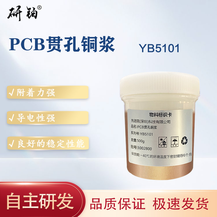
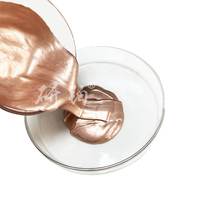
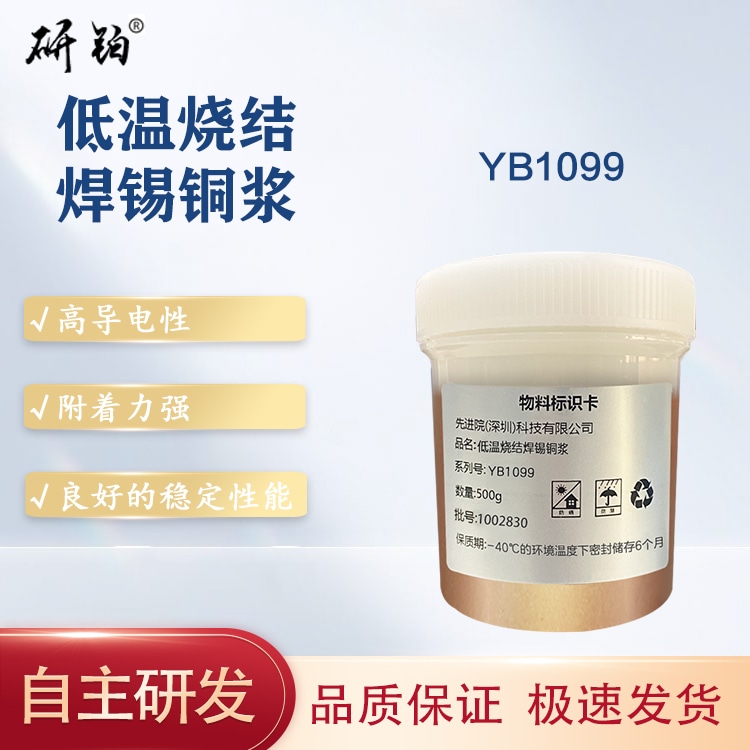
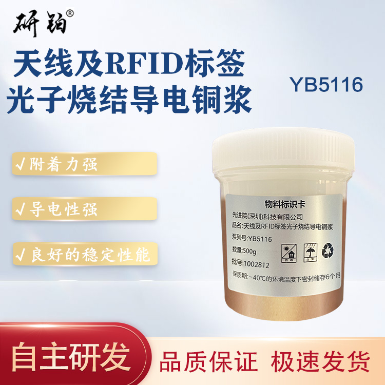
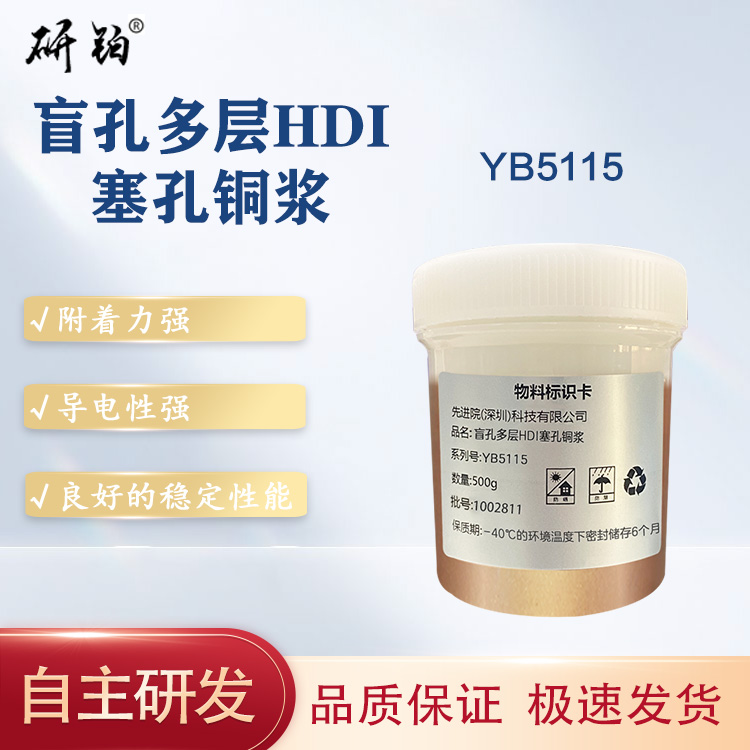
PCB through-hole copper paste is a high-performance conductive material designed specifically for through-hole conductive layers in the manufacturing process of printed circuit boards (PCBs). This copper paste is made by combining high-quality copper powder with a specially designed resin matrix, and is processed through fine mixing and dispersion techniques. It has excellent conductivity, heat resistance, and good adhesion, suitable for the production of conductive layers for PCB through holes, ensuring stable circuit connections.

Product characteristics
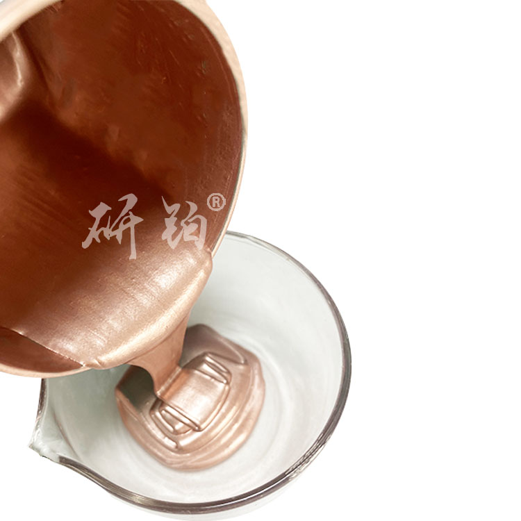
- High conductivity: The high content of copper powder ensures that the conductive layer has extremely low resistivity and improves conductivity.
- Heat resistance: able to maintain stable conductivity in high temperature environments, suitable for high-temperature processes in PCB manufacturing.
- Good adhesion: A strong bond is formed between the resin substrate and the PCB substrate, ensuring stable adhesion of the copper paste on the substrate.
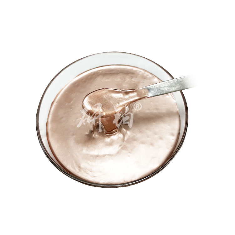
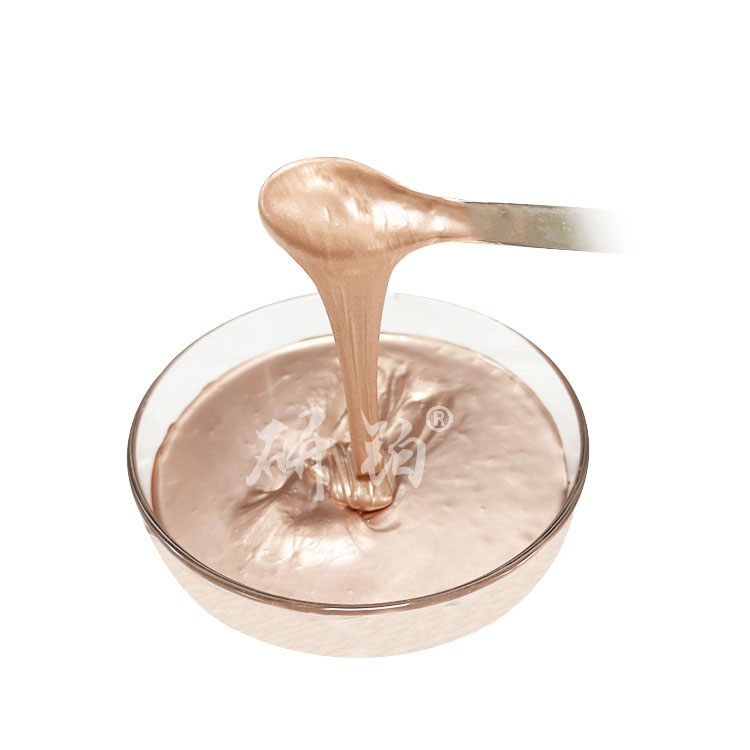
- Excellent processing performance: It has good fluidity and thixotropy, suitable for various processes such as screen printing and spraying.
- Environmentally friendly and pollution-free: Complies with environmental standards, with no harmful gas release during use, and is environmentally friendly.
Product advantages
- Improving conductivity: High copper content ensures excellent conductivity of the paste, meeting the requirements of PCB through-hole conductive layer.
- Enhanced heat resistance: able to maintain stable conductivity in high temperature environments, suitable for high-temperature processes.
- Improve adhesion: A strong bond is formed between the resin substrate and the PCB substrate, enhancing the stability of the copper paste.
- Cost reduction: Convenient processing performance reduces defects in the manufacturing process, helping to lower manufacturing costs.
- Environmentally friendly and pollution-free: The product meets environmental standards and does not release harmful gases during use, making it environmentally friendly.

application area
- Printed Circuit Board (PCB): A conductive layer material used for PCB through holes, providing high conductivity and good adhesion.
- Multilayer circuit board: suitable for through-hole conductive layers in multilayer circuit boards, ensuring stable connection of circuits.
- Other electronic components: Suitable for other electronic components that require high conductivity, heat resistance, and good adhesion.
workshop show


 en
en