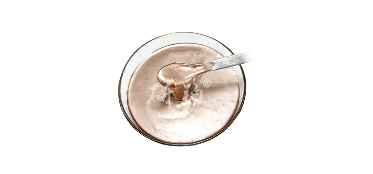
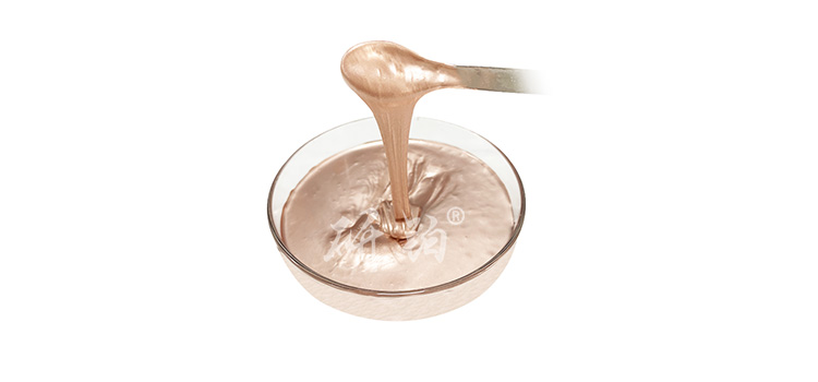
With the development of miniaturization, lightweight, and high-performance electronic devices, the design of printed circuit boards (PCBs) is facing unprecedented challenges. Especially for high-density interconnect (HDI) PCBs, how to effectively fill blind and buried holes has become an important step in improving PCB integration and signal integrity. As an effective means to solve this problem, the core of through-hole filling technology lies in selecting a suitable conductive copper paste. This article will provide a detailed introductionAdvanced Institute (Shenzhen) Technology Co., LtdSpecially developed for PCB through-hole fillingConductive copper pasteExplore its technical characteristics, formula, and application prospects.
Technical background
traditionalThrough hole fillingThe methods usually rely on electroplating or chemical plating techniques, but these two methods have certain limitations, such as electroplating requiring complex equipment and longer processing time, while chemical plating may lead to uneven coating problems. In order to solve these problems, Advanced Institute (Shenzhen) Technology Co., Ltd. has developed a new conductive copper paste that can be filled with through holes in a relatively short time through screen printing or injection filling, and has excellent conductivity and mechanical strength.
Technical characteristics of conductive copper paste
The conductive copper paste developed by Advanced Institute (Shenzhen) Technology Co., Ltd. has the following significant technical characteristics:
-
high conductivity
- Electrical resistivity: ≤ 20 μΩ·cm
- Volume resistivity: ≤ 18 Ω·cm
- Surface resistivity: ≤ 15 Ω/sq (100 μ m thick coating)
- This copper paste uses high-purity copper powder as the conductive phase, ensuring the conductivity of the material after curing, and is suitable for the conductivity requirements of high-density interconnect circuit boards.
-
fast curing
- Curing temperature: 150 ° C to 250 ° C
- Curing time: 30 minutes to 1 hour
- The rapid curing characteristic greatly shortens the production cycle and improves production efficiency. Meanwhile, low-temperature curing is also beneficial for protecting sensitive electronic components and avoiding damage caused by high temperatures.
-
Good filling performance
- Filling density: ≥ 95%
- Filling speed: ≥ 5 mm/min
- This copper paste has excellent fluidity and filling ability, which can effectively fill holes with diameters as small as 50 μ m, meeting the design requirements of high-density circuit boards.
-
Stable chemical properties
- Temperature resistance range:- 55 ° C to 260 ° C
- Resistance to moisture and heat aging: Tested for 1000 hours at 85 ° C/85% RH
- The conductive copper paste formula has been specially designed to have excellent chemical stability and can maintain its performance unchanged in harsh environments for a long time, enhancing the reliability of the PCB.
-
Environmentally friendly
- RoHS Compliance: Compliant with RoHS Directive requirements, does not contain harmful substances such as lead
- This product is a green and environmentally friendly product that meets international environmental standards and is suitable for use in various environments with strict environmental requirements.

formulation
The typical formula for conductive copper paste is as follows:
- Copper powder: High purity copper powder with a particle size range of 1 μ m to 5 μ m and a content of approximately 70% -80% (weight percentage).
- Organic carrier: containing resin and solvent, used to ensure the fluidity and printability of the slurry, with a content of about 15% -25% (weight percentage).
- Additives: including dispersants, binders and other auxiliary components, used to improve the performance of the slurry, with a content not exceeding 10% (weight percentage).
technological process
- Slurry preparation: Accurately weigh each component according to the formula and mix using a three roll machine or ball mill to ensure the uniformity of the slurry.
- Printing or filling: By using screen printing technology or injecting slurry into holes, a predetermined filling layer is formed.
- Drying: Perform preliminary drying at 80 ° C to 120 ° C to remove solvents from the organic carrier.
- Curing: High temperature sintering is carried out at a temperature of 150 ° C to 250 ° C to fuse copper powder and form a dense conductive layer.
- Trimming and testing: The filling layer is trimmed by laser or mechanical methods, and then subjected to appearance and performance testing.
application area
Developed by Advanced Institute (Shenzhen) Technology Co., LtdPCB through-hole filling with conductive copper pasteWidely used in the following fields:
- High density interconnect (HDI) PCB: suitable for high-density circuit boards in high-end electronic products such as smartphones, tablets, server motherboards, etc.
- RF and microwave components: used as conductive connection materials in RF filters, antennas, microwave integrated modules, and other equipment to improve signal transmission efficiency.
- Automotive electronics: applied to automotive radar systems, in vehicle communication devices, etc., supporting the trend of automotive intelligence.
- New energy industry: Improve the overall performance of systems in areas such as solar panels and electric vehicle battery management systems.
Performance Verification
In order to verify the performance of conductive copper paste, the following tests were conducted:
- Conductivity test: The resistivity of the cured copper paste was measured under standard conditions, and the results showed excellent conductivity.
- Filling performance test: Observe the filled holes under a microscope to confirm that their filling density and speed meet expectations.
- Mechanical strength testing: The adhesion between copper paste and different substrates was tested using a tensile testing machine, and the results showed strong adhesion.
- Durability testing: Place the sample in a high-temperature and high humidity environment for aging testing to ensure its performance stability under extreme conditions.
conclusion
With the continuous development of electronic technology, the requirements for PCB materials will become increasingly high. The PCB through-hole filling conductive copper paste developed by Advanced Institute (Shenzhen) Technology Co., Ltd. has brought new solutions to the industry with its unique technical advantages and excellent performance. In the future, with the advancement of materials science and optimization of production processes, we have reason to believe that this conductive copper paste will play an important role in more fields, driving PCB technology to new heights.