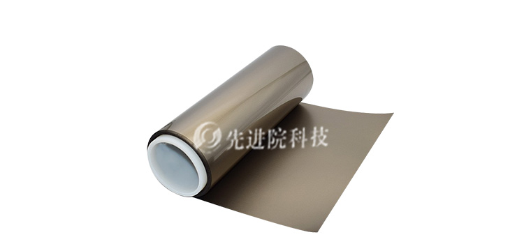
Advanced Institute (Shenzhen) Technology Co., Ltd.: Exploring the Path of Lightweight Design for Graphene Absorbing Materials
In today's era of rapid technological development, the widespread use of electronic devices has made electromagnetic pollution and interference problems increasingly prominent, and the research and development of absorbing materials has become the key to solving this problem. Graphene, as a new type of carbon based material, has shown great potential in the field of absorbing materials due to its unique advantages such as lightweight, high conductivity, large specific surface area, and strong dielectric loss. However, traditional graphene absorbing materials often have the problem of large thickness, which limits their application in some fields that require high weight and space. Advanced Institute (Shenzhen) Technology Co., Ltd. actively engages in the research and development of graphene absorbing materials, committed to reducing their thickness to achieve lightweight design. The following are the company's explorations and practices in this area.
1、 In depth study of graphene properties and optimization of material microstructure
The research team of Advanced Institute (Shenzhen) Technology Co., Ltd. is well aware that in order to achieve lightweight design of graphene absorbing materials, the key is to deeply understand the characteristics of graphene and optimize its microstructure. Graphene has a unique two-dimensional structure and excellent electrical properties, but its impedance matching performance is poor, which limits its absorption efficiency and often requires a larger thickness to achieve the desired absorption effect.
To address this issue, the team improved the impedance matching characteristics of graphene by doping it with heterogeneous elements and designing its morphology structure. For example, doping graphene with elements such as nitrogen and boron can alter its electronic structure and electromagnetic properties, allowing electromagnetic waves to enter the material more effectively and be absorbed. At the same time, graphene can be prepared into low dimensional structures such as nanosheets and nanotubes to increase the specific surface area and interface polarization of the material, thereby improving its absorption performance. By optimizing these microstructures, the required thickness of the material has been effectively reduced while ensuring the absorption effect.
2、 Develop new composite materials and leverage synergistic effects
When the thickness of a single graphene absorbing material is reduced, its absorbing performance often fails to meet practical needs. Therefore,Advanced Institute (Shenzhen) Technology Co., LtdActively exploring the development of new composite materials, combining graphene with other materials with absorbing properties to achieve synergistic effects and achieve lightweight design.
The company's researchers composite graphene with magnetic materials such as ferrite and magnetic metal micro powders. Magnetic materials have good magnetic loss characteristics, which can complement the dielectric loss characteristics of graphene, broaden the absorption frequency band, and improve absorption efficiency. In the composite process, by precisely controlling the proportion and distribution of materials, both materials can fully leverage their respective advantages and achieve good absorption effects at thinner thicknesses.
In addition, the company is also attempting to composite graphene with conductive polymers. Conductive polymers have good flexibility and processing properties. By adding conductive fillers such as carbon nanotubes, graphene, etc., their absorption performance can be significantly improved. After composite with graphene, not only can the electromagnetic properties of the material be further optimized, but the density of the material can also be reduced, achieving lightweighting.
3、 Innovative preparation process to achieve precise control
Preparation process forGraphene absorbing materialThe thickness and performance have a crucial impact. Advanced Institute (Shenzhen) Technology Co., Ltd. continuously innovates preparation processes to achieve precise control of material thickness.
The company adopts advanced nanotechnology, such as atomic layer deposition (ALD), chemical vapor deposition (CVD), etc., to precisely grow graphene and other absorbing materials on the substrate. These technologies can achieve precise control at the atomic level and prepare absorbing materials with uniform thickness and dense structure. By adjusting the process parameters, the thickness of the material can be precisely controlled to minimize its absorption performance while meeting the requirements.
At the same time, the company has also developed a multi-layer composite preparation process to prepare absorbing materials by stacking graphene based composite materials with different properties layer by layer. Each layer of material absorbs electromagnetic waves of different frequencies, and by designing the thickness and performance of each layer of material reasonably, efficient wideband absorption can be achieved at a relatively thin total thickness.
4、 Customized design based on practical application needs
Advanced Institute (Shenzhen) Technology Co., Ltd. fully recognizes that there are differences in the thickness and performance requirements of graphene absorbing materials in different application fields. Therefore, the company conducts customized design based on actual application needs.
In the aerospace industry, there is a high demand for lightweight materials. The company has developed an ultra-thin graphene absorbing material to meet this demand. By optimizing the material formula and preparation process, the material thickness is reduced to the extreme while ensuring good absorbing performance in a specific frequency range, meeting the electromagnetic shielding and stealth requirements of aerospace equipment.
In the field of wearable devices, in addition to lightweight requirements, materials also need to have good flexibility and comfort. The company has developed a flexible graphene absorbing material, which can maintain good flexibility and absorption performance even with thin thickness by selecting suitable substrate materials and preparation processes, providing an effective solution for electromagnetic protection of wearable devices.
5、 Looking ahead to the future
Advanced Institute (Shenzhen) Technology Co., Ltd. has achieved significant results in reducing the thickness of graphene absorbing materials to achieve lightweight design. However, with the continuous development of technology and the increasing demand for applications, the company still faces many challenges. In the future, the company will continue to increase research and development investment, conduct in-depth research on the performance and preparation process of graphene absorbing materials, continuously explore new material systems and design methods, and strive to achieve lighter weight, higher performance, and wider application of graphene absorbing materials. We believe that with the unremitting efforts of Advanced Institute (Shenzhen) Technology Co., Ltd., graphene absorbing materials will play an important role in more fields and make greater contributions to solving electromagnetic pollution and interference problems.
 en
en 


