1、 Introduction
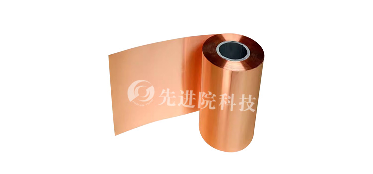
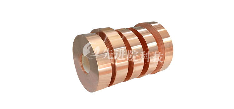
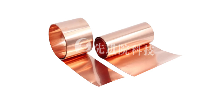
PI copper plated film, as an important functional material, has broad application prospects in many fields such as flexible circuit boards and electromagnetic shielding. Its conductivity is one of the key factors determining its application efficiency, and the thickness of the copper layer, as a controllable parameter, has a crucial impact on its conductivity. Advanced Institute (Shenzhen) Technology Co., Ltd. has been committed toPI copper plated filmThe research and innovation of related technologies provide strong support for a deeper understanding of their performance relationships.
2、 Experimental section
(1) Experimental materials and sample preparation
The experiment adopts
Advanced Institute (Shenzhen) Technology Co., LtdThe independently developed PI film as the substrate material has excellent high temperature resistance, mechanical properties, and chemical stability. The copper coating is prepared using electroplating technology, and a series of PI copper plating film samples with different copper layer thicknesses are prepared by precisely controlling parameters such as electroplating time and current density. The thickness range of the copper layer is set to 1-10 microns to ensure coverage of different application scenarios from thinner to thicker.

(2) Testing method
- Copper layer thickness measurement
Using high-precision film thickness measuring instruments, such as X-ray fluorescence thickness gauges (XRF), to accurately measure the copper layer thickness of PI copper plated film samples. This instrument can quickly and accurately measure the thickness of copper layer non destructively, with a measurement accuracy of ± 0.1 microns, providing a reliable data basis for subsequent analysis.
- Conductivity testing
Measure the electrical resistivity of PI copper plated film using the four probe method to characterize its conductivity. The four probe method can effectively eliminate the interference of contact resistance and accurately measure the bulk resistance of materials. During the measurement process, ensure good contact between the probe and the sample surface, and control the measurement environment temperature at 25 ± 2 ℃ and humidity at 40% -60% to reduce the influence of environmental factors on the measurement results.
3、 Results and Discussion
(1) The influence of copper layer thickness on electrical resistivity
As the thickness of the copper layer gradually increases from 1 micron to 10 microns,
PI copper plated filmThe resistivity shows a clear downward trend. When the thickness of the copper layer is thin, such as 1-3 microns, the resistivity is relatively high. This is because at this time, there are relatively few electron conduction paths in the copper layer, and the electron scattering phenomenon is more severe, which limits the effective transmission of current. As the thickness of the copper layer increases to 5-7 microns, the decrease in resistivity gradually increases, the number of electron conduction paths increases, and the migration of electrons in the copper layer becomes smoother, resulting in a significant improvement in conductivity. When the thickness of the copper layer reaches 8-10 microns, the decreasing trend of resistivity tends to be gentle, indicating that the effect of increasing the thickness of the copper layer on improving conductivity gradually weakens.

(2) Microstructure analysis
The microstructure of PI copper plated films with different copper layer thicknesses was observed by scanning electron microscopy (SEM). As a result, it was found that when the copper layer was thinner, the copper grains were smaller and relatively unevenly distributed, with more grain boundaries. Electrons would scatter when passing through the grain boundaries, thereby affecting the conductivity. As the thickness of the copper layer increases, the copper grains gradually grow and tend to be evenly distributed, the grain boundaries decrease, and the obstacles to electronic conduction decrease, which is consistent with the trend of changes in electrical resistivity. Advanced Institute (Shenzhen) Technology Co., Ltd. further found in its research that by optimizing the electroplating process parameters, the growth direction and size of copper grains can be controlled to a certain extent, thereby further improving the conductivity of PI copper plated films.
4、 Theoretical analysis
From a theoretical perspective, according to classical electron transport theory, the resistivity of materials is closely related to the scattering mechanism of electrons. exist
PI copper plated filmWhen the copper layer is thin, surface scattering and grain boundary scattering play a dominant role, resulting in higher electrical resistivity. As the thickness of the copper layer increases, the average free path of electrons increases, the scattering probability decreases, and the conductivity is improved. When the thickness of the copper layer reaches a certain level, internal defect scattering and impurity scattering become the main factors affecting the resistivity, and the correlation between these factors and the thickness of the copper layer is relatively weak, so the resistivity changes tend to flatten out.

5、 Conclusion
Through experimental research and theoretical analysis, it has been clarified that
PI copper plated filmThe relationship between conductivity and copper layer thickness. When the thickness of the copper layer is thin, the conductivity is poor. As the thickness of the copper layer increases, the conductivity significantly improves. When the thickness reaches a certain value, the improvement effect gradually weakens. The research results of Advanced Institute (Shenzhen) Technology Co., Ltd. provide important reference for the design of copper layer thickness of PI copper plating film in practical applications, which helps to promote the further application and development of this material in flexible electronics, electromagnetic shielding and other fields, and provides strong technical support for the technological upgrading of related industries.
The above data is for reference only, and specific performance may vary due to production processes and product specifications.
