
Hotline:0755-22277778
Tel:0755-22277778
Mobile:13826586185(Mr.Duan)
Fax:0755-22277776
E-mail:duanlian@xianjinyuan.cn
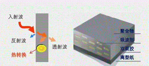
AbsorberIt is a composite material with excellent absorption ability for electromagnetic waves. This type of absorbing material is a composite material formed by physically refining and magnetic field processing an alloy to form a high permeability magnetic alloy, and uniformly dispersing it in a polymer. In engineering applications, in addition to requiring absorbing materials to have high absorption rates for electromagnetic waves in a wide frequency band, it is also required to have lightweight, temperature resistance, moisture resistance, corrosion resistance, and other properties.

Absorbing materials utilize metals with high magnetic permeability and high loss to crystallize into various soft magnetic alloys in ultrafine molecules, stacked with layer by layer strip thin films, and efficiently absorb microwave noise generated by electronic components, modules, and surface currents over a wide frequency range, providing excellent EMC solutions for various electronic devices. This type of absorbing material can achieve ultra-thin main application areas: clutter suppression and electromagnetic interference resistance in mobile phones, electronic equipment, high-frequency devices, microwave active devices, shielding boxes, radar and microwave communication systems. According to different application frequency bands, the thickness and formula of functional materials can be adjusted to make electromagnetic wave absorbing adhesives with different thicknesses and effects. The main principles are:
When a certain volume fraction of conductive particles is filled in the absorbing material, they come into contact with each other, forming a continuous state of electrons. When the external electromagnetic field reaches the outside of the conductive rubber, strong electromagnetic waves hit the free electrons of the conductive particles, causing them to move freely. During the movement, the free electrons form an electromagnetic field opposite to the external electromagnetic field, and the internal and external electromagnetic fields cancel each other out, achieving the effect of weakening electromagnetic interference waves;
Another principle of absorbing materials is energy conversion, the law of conservation of energy, where electromagnetic waves hit free electrons. During the movement of free electrons, due to the resistance of conductive particles, heat is generated, that is, electromagnetic interference waves - kinetic energy of free electron motion - thermal energy, to weaken electromagnetic interference waves.
The principle of absorbing materials is mainly based on magnetic microwave absorbers, which convert the electromagnetic waves emitted by electronic devices into thermal energy through insulation loss, magnetic loss, and impedance loss to reduce electromagnetic radiation. They have the characteristics of high magnetic permeability, wide selectable frequency band, and can be developed specifically for specific frequency bands.
Absorbing materials have good absorption characteristics in the range of 10MHz~6GHz, which can avoid electromagnetic interference or leakage caused by secondary reflection. The products are mainly of the absorbing patch type and can also be processed into various shapes according to customer needs. Wave absorbing plates can be used inside electronic device cavities such as laptops, mobile phones, and communication cabinets.
AbsorberGood electromagnetic wave absorption effect, wide absorption frequency, customizable products according to customer frequency requirements, thin thickness, high cost-effectiveness, wide range of applications and applicability. The full English name of RFID is Radio Frequency Identification, also known as electronic tags, Radio Frequency Identification, inductive electronic chips, proximity cards, proximity cards, contactless cards, and electronic barcodes. RFID radio frequency identification is a non-contact automatic identification technology that automatically identifies target objects and obtains relevant data through radio frequency signals. The identification work does not require manual intervention and can work in various harsh environments. RFID technology can recognize high-speed moving objects and simultaneously identify multiple tags, making operation fast and convenient. Short distance RF products are not afraid of harsh environments such as oil stains and dust pollution, and can replace barcodes in such environments, such as tracking objects on factory assembly lines. Long range RF products are commonly used in transportation, with recognition distances of up to tens of meters, such as automatic toll collection or vehicle identification.

After more than ten years of development, China's RFID industry has become relatively mature in technology, especially in the past two years. Against the backdrop of the country's active encouragement and vigorous promotion of the healthy development of the industry, with the continuous promotion of various factors on the Internet of Things, it has maintained a steady upward trend in development. The industry has also reached a consensus on the development of frequency standards for RFID. At present, the commonly used frequency internationally is 13.56MHz. The high-frequency RFID technology of 13.56MHz is widely used in public transportation cards and mobile payments, especially in South Korea, Japan and other places, due to its stable performance, reasonable price, and matching reading distance range with the actual application distance range. RFID electronic tags are often used in metal environments. When RFID electronic tags are close to metal, due to the strong reflectivity of metal to electromagnetic waves, the signal will weaken and the card reading distance will become closer. Severe interference will result in card reading failure. The current common solution is to stick a layer of absorbing material on the back of electronic tags.AbsorberIt has been widely used in various aspects such as noise reduction, absorption, and EMC in electronic devices, and experts have also made many models to explain its working principle, forming a lot of theoretical knowledge. However, the disadvantage is that these theories are relatively complex, and some readers outside the field find it difficult to understand. Based on the various problems encountered by many engineers in their usage, this article will take the use of absorbing materials in 13.56MHz passive RFID systems as an example and explain it in simple, easy to understand, and accessible language, hoping to provide readers with some help.
1. The composition of RFID system
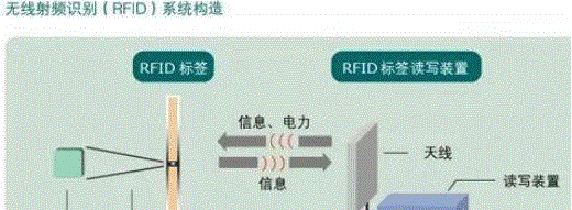
The RFID system consists of an electronic tag or non-contact smart card (such as a smart phone with card swiping function) placed on the recognized object, and a device that sends instructions to the electronic tag and collects feedback information from the electronic tag. The device is also known as an RFID card reader or reader. As shown in Figure 1, in order to enable other devices to display or use this data, an external interface with RS232 protocol can generally be added to the reader/writer, so that information can be transmitted with external devices.
So passive electronic tags require the energy needed for the chip and memory to work, which needs to be provided by the reader/writer. The communication between the reader/writer and the electronic tag is achieved through the principle of electromagnetic coupling, and the energy of the electronic tag is generated by the coil antenna of the reader/writer through electromagnetic coupling.
The high-frequency electromagnetic field is generated by the antenna coil of the reader/writer, and then the magnetic field passes through the cross-section of the coil and the space around the coil. According to the tag's usage frequency of 13.56MHz and wavelength of 22.1m, which is much greater than the distance between the reader antenna and the electronic tag, the electromagnetic field between the reader antenna and the antenna can be treated as a simple alternating magnetic field.
By adjusting the antenna coil and capacitor of the electronic tag to form a resonant circuit, tuned to the designated transmission frequency of 13.56MHz of the reader/writer, the voltage generated on the inductance of the coil in the tag reaches the maximum value according to the resonance of the circuit. The power transmission efficiency between the antenna coil of the reader and the electronic tag is proportional to the number of turns of the coil in the tag, the area enclosed by the coil, the relative angle between the two, and the distance between them. This is also the reason why RFID tags have a certain limit on the reading distance.
For RFID electronic tags used at 13.56MHz, their maximum read and write distance is usually around 10 centimeters, and the chip's current consumption is approximately 1mA. As the frequency increases, the required inductance of the electronic tag coil decreases in the number of turns, typically ranging from 3 to 10 turns at that frequency.
The reading distance of RFID tags is not only related to themselves, but also to their environment. When using inductively coupled radio frequency identification systems, it is often required to directly install the antenna of the reader or electronic tag on a metal surface. However, it is impossible to directly install magnetic antennas on metal surfaces.
Because the magnetic flux of the antenna passing through the metal surface will generate induced eddy currents, according to Lenz's law, eddy currents will have a counter effect on the field of the antenna and rapidly attenuate the magnetic field on the metal surface. As a result, the data reading distance between the reader and the electronic tag will be severely affected, and there may even be misreading or reading failure. Whether the magnetic field generated by the coil installed on the metal surface itself or the field approaching the metal plate from the outside (electronic tags on the metal surface), the result is the same.
2. The absorption principle of absorbing materials in RFID
Absorbing materials are a type of material with high magnetic permeabilityMagnetic functional materialsIt is usually made by uniformly filling some absorbents onto polymer materials and using special processes. Compared with traditional absorbing materials, this type of high-performance absorbing material for 13.56MHz has different performance characterization and usage principles. Traditional absorbing materials are mainly used in military confrontations to cover up and confuse enemy radar reconnaissance aircraft, warships, and armored tanks. They have a high frequency of use in the microwave range and are analyzed using far-field models. The absorbing materials mentioned in this article mainly target the magnetic conductors used in civilian electronic devices to provide a path for magnetic fields. They have the characteristics of high magnetic permeability and low magnetic loss at the operating frequency, and increased loss above the operating frequency. They have the properties of low-pass filters. However, due to its advantages such as flexibility and easy installation, it has been increasingly favored by R&D engineers.
Let's compare the special applications of absorbing materials in electronic tag products and solve the problem of communication failure when electronic tags encounter metal plates.
a) It indicates that a non-metallic and non-magnetic object is not significantly affected by the propagation of electromagnetic fields, and still follows the original direction, which is equivalent to the propagation of electromagnetic waves in free space, so the energy and direction of the electromagnetic field are not disturbed. And Figure 3 (b) shows a metal plate with good conductivity attached on the basis of Figure 3 (a). It can be clearly seen in the figure that the direction of magnetic field lines has undergone a significant change. The main manifestation is the change in magnetic field before and after the metal plate, which is called shielding phenomenon.
There is no magnetic field behind the metal plate, and the direction facing the incident electromagnetic field will also generate an electromagnetic field opposite to the direction of the incident electromagnetic field due to the eddy current generated by the metal plate, thereby weakening the magnetic field and even completely canceling out the original magnetic field. This problem can be solved by the solution shown in Figure 3 (c), which is to attach an absorbing material (sheet) to the surface of the metal plate facing the direction of the incident electromagnetic field, effectively providing an effective path for magnetic field transmission. Therefore, due to the presence of the absorbing material, the eddy current effect of the metal plate is effectively avoided.
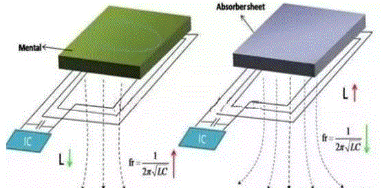
Similarly, when the RFID electronic tag approaches the metal sheet, as shown in Figure 4 (a), a similar effect will occur. At the same time, the resonant frequency fr of the coil will also change, and fr will move towards lower frequencies. At this time, the communication capability of the electronic tag will greatly decrease, and the card reading distance will be severely interfered with.
By inserting a highly magnetic material between the coil and the metal surface, as shown in Figure 4 (b), the generation of eddy currents can be largely avoided, allowing electronic tags to be used with confidence on the metal surface. When installing the antenna on a magnetic sheet, it should be noted that the inductance of the loop coil antenna will significantly increase due to the high magnetic permeability of the magnetic material, requiring a readjustment of the resonant frequency or a matching network (which needs to be re determined inside the reader/writer).

3. Conclusion
With the increasingly strict international standards for electromagnetic interference control, China has also aligned with international standards and accelerated the control of electromagnetic noise, especially in electronic products. Therefore, how to achieve electronic products meeting these requirements will be an important course. After years of development, absorbing materials have made great progress. However, with the increasing demand for electronics, absorbing materials will also develop towards thinner thickness, higher performance, and lighter weight under the premise of higher frequency of use. This is also the driving force behind material progress.

Advanced Institute (Shenzhen) Technology Co., Ltd, © two thousand and twenty-onewww.avanzado.cn. All rights reservedGuangdong ICP No. 2021051947-1 © two thousand and twenty-onewww.xianjinyuan.cn. All rights reservedGuangdong ICP No. 2021051947-2