Shielding materials for double-sided PCB wiring and flooring in electronic productsThermal conductive material AbsorberDesign is a method adopted by many design engineers for low-cost IoT and smart products; Due to the need for high-frequency operation of MCU/CPU driven by crystal oscillators in the product system; PCB flooring design can bring advantages to system EMC design!
What are the effects of copper flooring on EMI?
Theory and Analysis of 02 Double sided PCB System Flooring
1. Good flooring:
-
Pay attention to the routing of signal lines on the edge of the PCB board if laid on the ground; The external signal coupling of this signal line is reduced; There should be copper flooring at the edges of the PCB board;
-
Laying copper between signal lines can reduce crosstalk between signals, and EMI radiation in crosstalk is indirectly related to it!
If both can achieve or achieve EMI effect, it will be better! Paving is not measured by area in every place, it needs to be done with a goal in mind to have a good effect!
2. My viewpoint:
PCB has conditions for copper plating, and this copper plating is effective if it can improve EMI performance; It is recommended to use the rule of laying copper on the PCB floor!
3. Precautions:
To lay the ground in this design, it is necessary to ensure that the impedance between the signal laying plane and the system's reference ground potential is sufficiently small; Otherwise, this flooring will have an impact on radiation interference or anti radiation interference!

03 Practical Case Sharing
For high-frequency applications in electronic product circuits; Due to the interference of common mode current EMI in the system, we need to add a common mode inductor and its combination LCM * C EMI filter design at the DC-DC DC current output end and the interface connector end of the functional circuit; At this point, the layout and wiring of copper on the PCB will have an impact on our high-frequency EMI; The analysis parameters are as follows:
analysis:
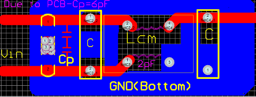
When there is a filtering design with common mode inductance in electronic circuits, there will be a coupling capacitance Cp between the wiring of the TOP layer and the PCB grounding of the bottom layer of the BOTTOM when the PCB grounding design is carried out in the front and rear stages; High frequency interference signals will affect the noise impedance performance of common mode inductors through coupling capacitors; The equivalent circuit is as follows:
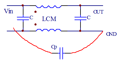
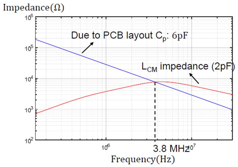
For example, the stray capacitance of the LCM device in the system design is 2pF; Its resonant frequency is around 4MHz; Due to the wiring of the PCB, there is a coupling capacitance parameter of 6pF between the input wiring and the copper ground of the PCB; After the resonance point of its LCM, its impedance value will decrease - as shown in the frequency impedance characteristic curve reference data in the above figure; During EMI testing, there may be issues with high-frequency EMI exceeding 4MHz!
3. When designing PCB double-sided board wiring with copper flooring; Improving PCB layout and routing in certain circuit designs can reduce high-frequency EMI electromagnetic interference; The reference for simple optimized PCB design is as follows:
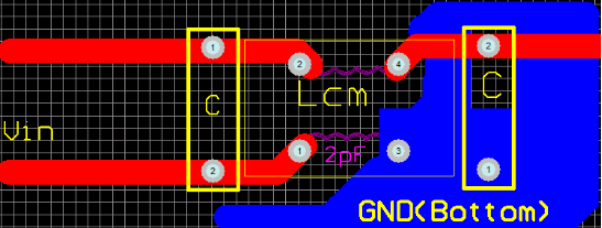
Attention: If there is a noise coupling source in the grounding layer, the grounding layer should not be close to sensitive input circuits.
04 Summary
For the copper flooring of PCB double-sided boards, it is not laid in every place according to the area. The flooring needs to be laid with a goal in order to have a good effect. Incorrect flooring design can actually deteriorate the EMC performance of the system.
 en
en 


