
Hotline:0755-22277778
Tel:0755-22277778
Mobile:13826586185(Mr.Duan)
Fax:0755-22277776
E-mail:duanlian@xianjinyuan.cn
With the trend of the electronics industry towards higher integration and smaller size, the requirements for materials are also increasing. Polyimide (PI) films are widely used in flexible circuit boards (FPCs) and other high-tech fields due to their excellent electrical properties, heat resistance, and mechanical strength. Coating an ultra-thin copper layer on the surface of PI film is one of the key processes for manufacturing flexible circuit boards. This article will explore the special difficulties encountered in this process and propose corresponding solutions.
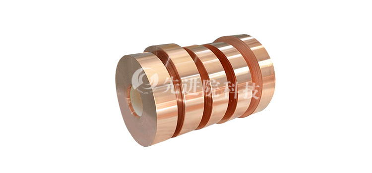
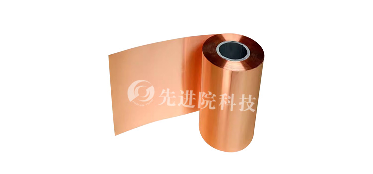
Advanced Institute (Shenzhen) Technology Co., LtdFocusing on the research and development of polymer materials and their composites, especially inPI copper plated filmWe have accumulated rich experience in production. However, ensuring the uniformity and continuity of the copper layer during the production process, especially when the thickness reaches the micrometer or even sub micrometer level, remains a challenge.
When depositing an ultra-thin copper layer on a PI film, the flexibility and thickness differences of the film itself can easily lead to uneven distribution of the coating. Experimental data shows that in some areas where the thickness of the copper layer is only 0.05 μ m, if not properly controlled, local areas may experience insufficient or excessive thickness, which can affect the performance of the final product.
The continuity of the ultra-thin copper layer is another key indicator. In actual production, it has been found that when the thickness of the copper layer is less than a certain threshold (such as 0.1 μ m), problems such as pinholes or cracks are prone to occur, which can seriously affect the conductivity of the copper layer. Through microscopic observation, it can be found that there are obvious defects in some areas, which can lead to a decrease in the qualification rate of the finished product.
The adhesion between PI film and copper layer is also an important consideration in production. If the adhesion is poor, it is easy to peel off during subsequent processing, thereby affecting product quality. Experiments have shown that specific pretreatment processes, such as plasma treatment, can significantly improve the adhesion between PI thin films and copper layers.
The plating process for producing ultra-thin copper layers often requires finer operating conditions and higher technical requirements, which also means higher production costs. Therefore, while ensuring product quality, how to effectively control costs and improve production efficiency is a problem that manufacturers need to consider.
In response to the above difficulties, Advanced Institute (Shenzhen) Technology Co., Ltd. has put forward the following suggestions:
After implementing the above improvement measures, the experimental results showed that the uniformity and continuity of the copper layer were significantly improved, and the pinhole rate decreased from 5% to below 1%; At the same time, the adhesion between the copper layer and the PI film has also been significantly improved, and the peel strength has increased by about 30%.
In summary, although in productionPI copper plated filmAt present, the plating process of ultra-thin copper layers faces many challenges, but these problems can be effectively solved through technological innovation and process optimization. Advanced Institute (Shenzhen) Technology Co., Ltd. will continue to be committed to technology research and development, promoting the continuous progress and development of the industry.

Advanced Institute (Shenzhen) Technology Co., Ltd, © two thousand and twenty-onewww.avanzado.cn. All rights reservedGuangdong ICP No. 2021051947-1 © two thousand and twenty-onewww.xianjinyuan.cn. All rights reservedGuangdong ICP No. 2021051947-2