
Hotline:0755-22277778
Tel:0755-22277778
Mobile:13826586185(Mr.Duan)
Fax:0755-22277776
E-mail:duanlian@xianjinyuan.cn
As the core component of modern electronic devices, the development of PCB (printed circuit board) design and manufacturing technology is crucial for improving the performance of electronic devices.Copper paste through holePCB board, as a special type of PCB board, its unique copper paste through-hole technology has significantly improved the performance of circuit boards. This article will provide an in-depth analysis of the technical characteristics, manufacturing process, and applications of copper paste through-hole PCB boards by Advanced Institute (Shenzhen) Technology Co., Ltd.
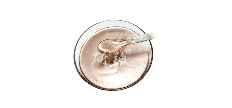
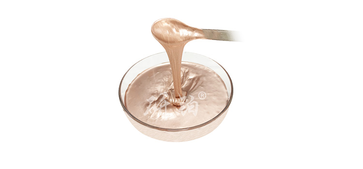
1. Superior conductivity: Copper paste through-hole technology fills copper paste in the through-hole of PCB board, making the through-hole have excellent conductivity. This technology can effectively reduce the resistance of the circuit board and improve the current transmission efficiency of the circuit board.
2. Good heat dissipation performance: Copper, as an excellent thermal conductive material, can significantly improve the heat dissipation performance of PCB boards when filled in through holes. In high-power and high heat generating electronic devices, copper paste through-hole PCB boards can effectively reduce the operating temperature of the circuit board, improve the stability and reliability of the equipment.
3. Structural strength enhancement: Copper paste through-hole technology can also enhance the structural strength of PCB boards. Due to the formation of a sturdy structure after curing, copper paste filled in through holes can significantly improve the mechanical properties of PCB boards, such as bending resistance and vibration resistance.
1. Design circuit diagram: Based on the requirements of electronic devices, design a suitable circuit diagram, determine the connection method of the circuit and the position of components.
2. Making printed film: Convert the circuit diagram into printed film, which marks the position of the circuit pattern and components.
3. Substrate fabrication: Place the printed film on the substrate and transfer the circuit pattern onto it through photosensitive materials and ultraviolet exposure.
4. Etching: Place the substrate in an etching solution to etch away the unwanted parts, leaving behind the desired circuit pattern.
5. Drilling: Drilling holes in circuit patterns to leave space for component installation and copper paste filling.
6. Copper paste filling: Inject copper paste into the borehole, and use appropriate processes to solidify the copper paste in the through-hole and form a continuous conductive layer.
7. Installing components: Install the components at the drilled hole and connect them to the circuit through welding or other methods.
8. Testing: Test the PCB circuit board to ensure correct circuit connections and no issues such as short circuits or open circuits.
Copper paste through holePCB boards are widely used in various high-performance electronic devices due to their excellent conductivity, heat dissipation, and structural strength. For example, copper paste through-hole PCB boards play an important role in fields such as communication, computer, and industrial automation. Especially in high-power and high heat generating equipment, the advantages of copper paste through-hole PCB boards are more prominent, which can effectively improve the stability and reliability of the equipment.
Copper paste through-hole PCB board, as a high-performance type of circuit board, its unique copper paste through-hole technology has significantly improved the performance of the circuit board. With the continuous development of electronic technology, copper paste through-hole PCB boards will be applied and developed in more fields.

Advanced Institute (Shenzhen) Technology Co., Ltd, © two thousand and twenty-onewww.avanzado.cn. All rights reservedGuangdong ICP No. 2021051947-1 © two thousand and twenty-onewww.xianjinyuan.cn. All rights reservedGuangdong ICP No. 2021051947-2