
Hotline:0755-22277778
Tel:0755-22277778
Mobile:13826586185(Mr.Duan)
Fax:0755-22277776
E-mail:duanlian@xianjinyuan.cn
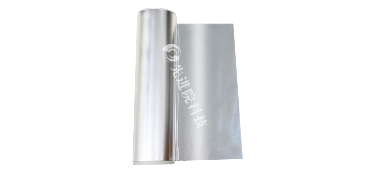
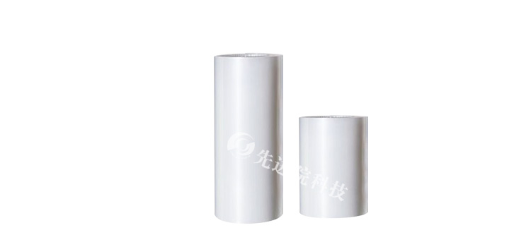
With the continuous advancement of technology, micro nano electronics and nanotechnology have become important components of modern information technology. These fields have extremely high requirements for material selection, especially in high-density integration, miniaturization, and multifunctionality. Polyimide (PI), as a high-performance organic polymer, plays an indispensable role in micro nano electronics. And when PI combines with metallic nickel to formNickel plated filmAt that time, it demonstrated a series of unique application advantages, providing new research and development directions for scientific research institutions and enterprises such as Advanced Institute (Shenzhen) Technology Co., Ltd.
PI itself has excellent thermal stability and can maintain good mechanical properties at temperatures above 200 ° C. After nickel plating, this temperature resistance characteristic is preserved or even enhanced, making PI nickel plating film an ideal choice for manufacturing microelectronic devices that operate in high-temperature environments. For example, in the aerospace industry, such materials can be used to protect sensitive components from extreme conditions.
PI nickel plating filmExhibiting excellent resistance to most chemical substances, including acidic and alkaline solutions, solvents, and corrosive gases. This not only extends the service life of the product, but also improves reliability, especially suitable for applications with harsh chemical environments, such as etching processes in semiconductor manufacturing.
Nickel is an excellent conductive material, and the continuous thin film formed on its surface can effectively reflect or absorb electromagnetic waves, providing excellent electromagnetic interference (EMI) shielding effect. This is crucial for wireless communication devices that require good signal integrity, such as the design of 5G base station antenna arrays.
By combining photolithography technology with electroplating processes, nickel structures at the micrometer or even nanometer level can be accurately deposited on PI substrates. This method allows for the manufacture of micro components with complex shapes, such as sensor probes, MEMS actuators, etc., meeting the needs of precision instrument manufacturing.
Some types of PI materials can achieve good biocompatibility after appropriate treatment, and the hardness and wear resistance conferred by the nickel layer make PI nickel plated composite materials suitable for the development of implantable medical devices, such as pacemaker lead cladding.
in summary,PI nickel plating filmWith its unique physical and chemical properties, it has demonstrated broad application prospects in the fields of micro nano electronics and nanotechnology. As one of the leading research institutions in China, Advanced Institute (Shenzhen) Technology Co., Ltd. is actively utilizing this innovative material to promote the development of related industries, and is committed to developing more efficient and reliable new generation electronic products and technological solutions.
The above data is for reference only, and specific performance may vary due to production processes and product specifications.

Advanced Institute (Shenzhen) Technology Co., Ltd, © two thousand and twenty-onewww.avanzado.cn. All rights reservedGuangdong ICP No. 2021051947-1 © two thousand and twenty-onewww.xianjinyuan.cn. All rights reservedGuangdong ICP No. 2021051947-2