
Hotline:0755-22277778
Tel:0755-22277778
Mobile:13826586185(Mr.Duan)
Fax:0755-22277776
E-mail:duanlian@xianjinyuan.cn
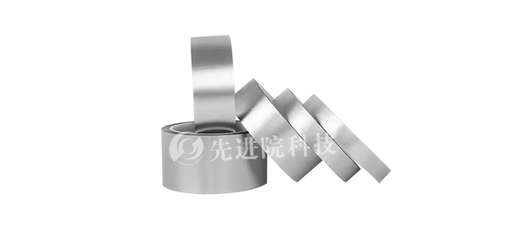
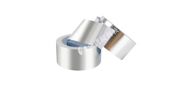
This article introduces polyimide (PI)Thin film copper plating and tin platingTechnology and its applications in electronics, semiconductors, and other high-tech fields. By customizing the coating thickness (12.5 μ m-25 μ m) and the unique properties of PI thin film tin coating, this article explores how this technology can meet the needs of different industries, and looks forward to its future application prospects and development trends.
Polyimide (PI) films are widely used in various industries due to their excellent physical and chemical properties. In recent years, with the development of copper and tin plating technology for PI thin films, this material has shown broader application prospects. Especially through customized coating thickness (12.5 μ m-25 μ m) andThin film tin plating processThe application greatly improves the performance and applicability of materials.
2.1 Basic Concepts
The PI film copper plating and tin plating technology refers to coating a layer of copper and a layer of tin on the surface of a polyimide film through a specific process to enhance the film's conductivity, weldability, and corrosion resistance.
2.2 Coating thickness can be customized
One of the biggest features of PI thin film copper plating and tin plating technology is the ability to customize the thickness of the coating according to specific application requirements, typically ranging from 12.5 μ m to 25 μ m. This feature greatly expands the application fields of PI thin films, enabling them to better adapt to various complex environments and high demand application scenarios.
3.1 PI thin film tin plated filmCharacteristics of
Conductivity: Tin plated film has good conductivity and is suitable for applications that require high electrical conductivity.
Weldability: Tin plating has excellent weldability, making it easy to assemble and connect electronic components.
Corrosion resistance: The tin layer can effectively protect the underlying material from oxidation and corrosion.
3.2 Application of PI thin film tin plated film
Electronics industry: used for making flexible circuit boards (FPC), integrated circuit (IC) packaging materials, etc.
Aerospace: Used as insulation material and conductive connector in high-temperature environments.
Automotive industry: used to manufacture battery modules and power system components for electric vehicles.
4.1 Process flow
Pre treatment: Remove impurities from the surface of PI film and improve its surface activity.
Primer: Apply a special primer layer on the PI film to enhance the adhesion between the metal layer and the film.
Copper plating: Using electroplating or chemical plating methods to deposit a copper layer on the surface of PI film.
Tin plating: Plating another layer of tin on top of a copper layer to provide the required conductivity and soldering performance.
4.2 Key technical points
Surface pretreatment technology: Ensure the cleanliness of the film surface and improve the adhesion of the coating.
Coating thickness control technology: By precisely controlling the parameters of the plating solution, ensure that the coating thickness meets the specified requirements.
Composite coating technology: achieving a tight combination of copper and tin layers, improving the stability of the overall structure.

5.1 Application Cases of Flexible Circuit Board (FPC)
In the product line of a certain electronic manufacturer, FPC made of PI thin film copper plated tin plated material exhibits excellent performance. These FPCs have been used in the folding area of mobile phone screens and have withstood hundreds of thousands of folding tests, demonstrating extremely high durability. In addition, due to the use of a specific thickness(12.5μm-25μm)The coating of FPC can also maintain good flexibility and conductivity.
The PI thin film copper plating and tin plating technology, with its unique performance advantages and wide application potential, has shown great development prospects in multiple fields such as electronics, semiconductors, aerospace, etc. With the advancement of materials science and technology, it is expected that this technology will be further optimized and improved in the coming years, bringing revolutionary changes to more high-tech industries. Especially with the continuous improvement of customized coating thickness (12.5 μ m-25 μ m) and thin film tin plating process, PI thin film copper plated tin plated materials will play an important role in higher demand application scenarios.

Advanced Institute (Shenzhen) Technology Co., Ltd, © two thousand and twenty-onewww.avanzado.cn. All rights reservedGuangdong ICP No. 2021051947-1 © two thousand and twenty-onewww.xianjinyuan.cn. All rights reservedGuangdong ICP No. 2021051947-2